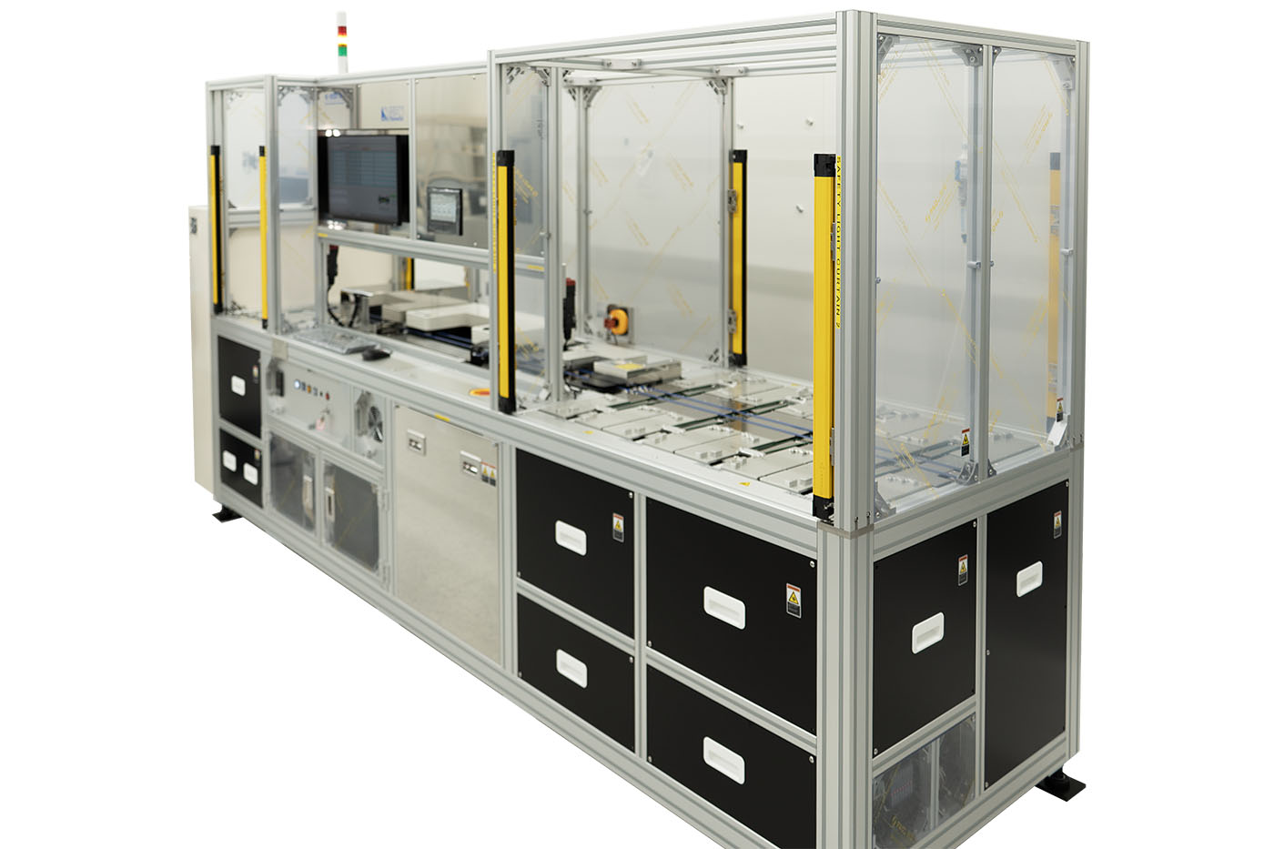
NC-6800FLA
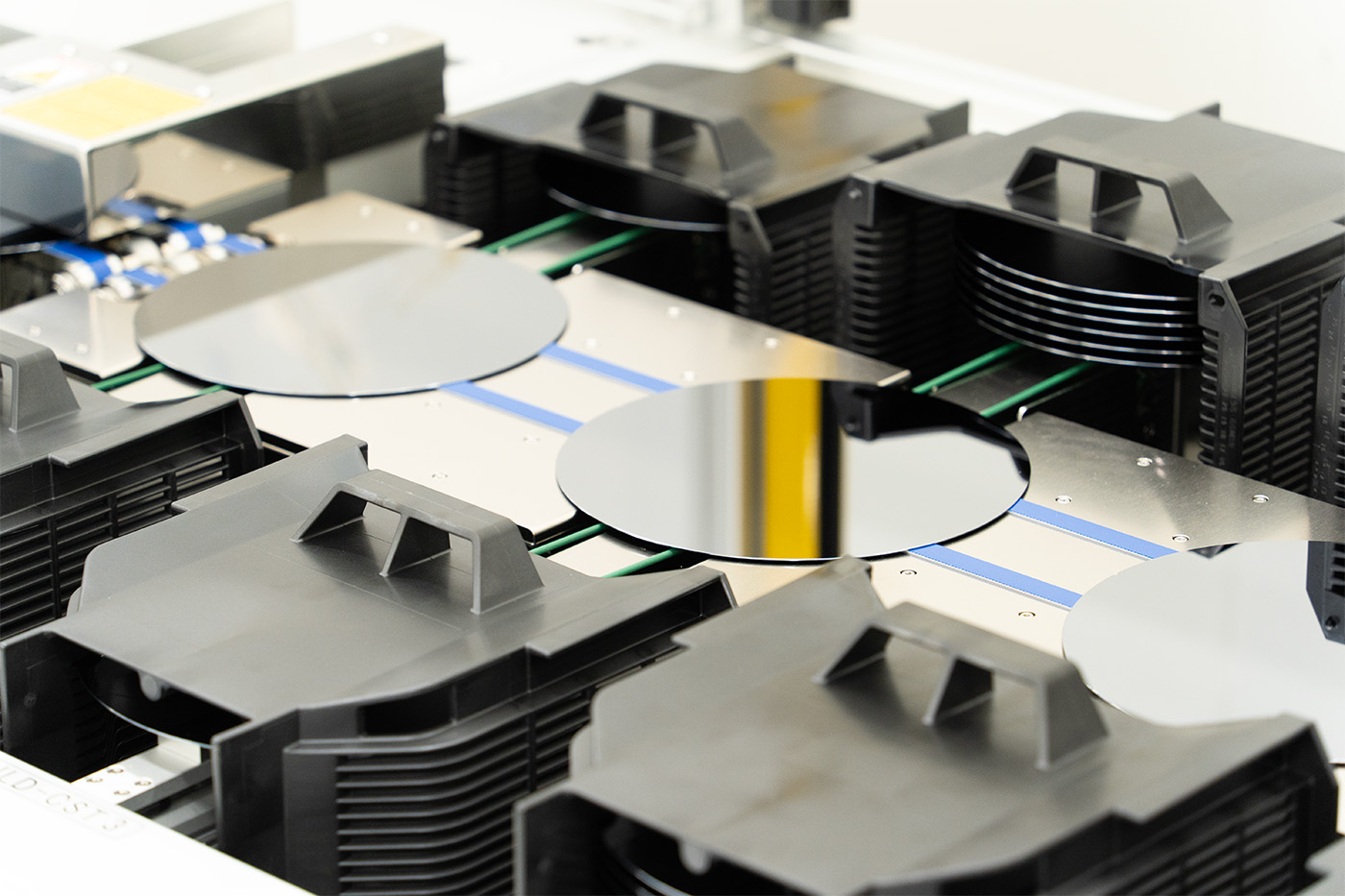
Fully automatic belt transfer sorting system by eddy current method (Non-contact)
Features
Non-contact measurement of resistivity, thickness and conductivity (P/N)
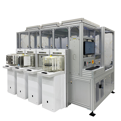
Number of cassette station can be changed by customers request
Eddy current method for resistivity, Electric capacitance method for wafer thickness
Temperature correction for silicon wafer function
Video
Details
Applications
- Semiconductor materials, Solar-cell materials (Silicon, Polysilicon, SiC etc)
Sample sizes
3 ~ 8 inch
Measuring range
[R] 1m ~ 200Ω・cm
[Thickness] 150 ~ 800μm (300μm between 150 and 800μm is recommended)
* The range is separated from each Low, Middle, High and S-High probe type.
*Please refer the measurement range for each probe type as below;
(1)Low:0.01~0.5Ω/□(0.001~0.05Ω·cm)
(2)Middle:0.5~10Ω/□(0.05~0.5Ω·cm)
(3)High:10~1000Ω/□(0.5~60Ω·cm)
(4)S-High:1000~3000Ω/□(60~200Ω·cm)
Non-Contact type resistance measurement
Fully automatic (with sample transfer system)
Product Information
Non-Contact type resistance measurement
Products Lineups
-
 Contact type resistance measurement
-
 Non-Contact type resistance measurement
-
 Lifetime measurement
-
 Flatness/Thickness measurement
-
 Spreading resistance measurement
-
 PN type checker
-
 4 point probe head
-
 Resistivity Reference wafer
Measurement principles & methods of Resistance Download by PDF file
*If you want PDF file [Measurement principles & methods of Resistance], please click here.


